Optiver FPGA Engineer Interview: Hardware Assessment and Low-Latency Design Preparation
Quick Overview
Use official Optiver FPGA role evidence and original timing, CDC, and packet-path exercises to prepare hardware assessment reasoning and low-latency design discussions.
For an Optiver FPGA Engineer interview, prepare to defend both correctness and speed. Reading RTL, recognizing hardware structures, and calculating timing are part of that preparation. Practice explaining why a design choice improves a real packet path without losing data, breaking clock-domain assumptions, or moving the bottleneck elsewhere.
This guide connects hardware-assessment preparation to two original exercises: a pipeline comparison and a packet-path review. For the wider trading-system context, use PracHub's low-latency trading infrastructure question, treating it as cross-role practice rather than an FPGA assessment prediction.
Evidence boundary: Official Optiver role information supports the engineering scope. Candidate reports describe particular experiences, not a universal current assessment format. The numerical examples, timing assumptions, and packet contract below are original preparation material. They are not Optiver performance figures, questions, or pass thresholds.
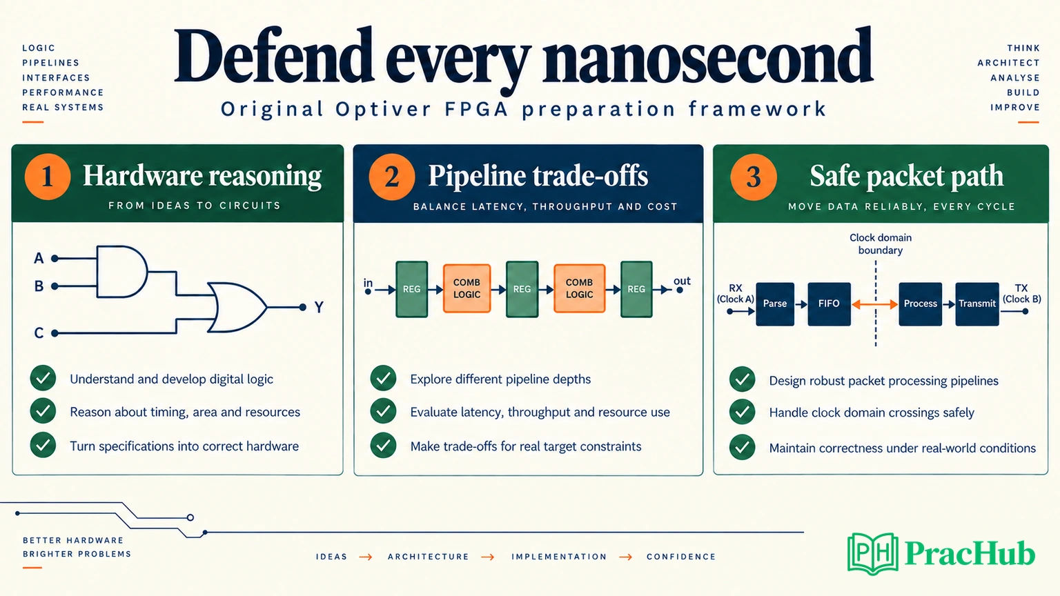
What the official Optiver FPGA role tells you
Official role evidence: The Chicago Graduate FPGA Engineer opening for a 2027 start describes high-speed hardware for network infrastructure and trading components, parallel processing, low-level networking, and collaboration with traders, software developers, and infrastructure engineers. It asks for hands-on FPGA or ASIC design and experience with VHDL, Verilog, or SystemVerilog. Its stated graduation window is December 2026 through June 2027. These are requirements for that opening, not every Optiver FPGA position. Official graduate posting
The posting also describes an eight-month reapplication restriction after participating in an FPGA graduate or internship assessment or interview at any location. Check the current posting and recruiter guidance before reapplying; do not assume a different office resets eligibility.
Preparation inference: Practice reasoning about a data path from input acceptance to output availability. Be ready to explain the hardware you inferred, its bottleneck, and how you verified the result. Do not borrow the trading mental-math assessment or the software-engineer object-oriented coding format simply because the employer is the same.
Hardware assessment: what reports support and what remains uncertain
Candidate report: An August 2026 public account describes completing an FPGA assessment with digital-logic reasoning, HDL interpretation, and a coding component. In a follow-up, the author links an Amsterdam internship opening. This is internship evidence, not confirmation of the Chicago graduate format. Candidate account
Other recent discussions mention similar fundamentals, but some are preparation requests or replies without a completed-loop account. Reports also differ in how they describe the permitted HDL. Two independently verified same-cycle accounts establishing the exact graduate assessment were not found in this review.
Use your invitation to confirm language, sections, timing, navigation, and allowed tools. Historical 2025 timers should not become a fixed 2027 schedule. Likewise, someone finding an assessment easy does not establish a cutoff or imply that later interviews will be easy.
As preparation recommendations, work on truth tables, Boolean simplification, combinational versus sequential behavior, register inference, reset behavior, and timing calculations. Explain the reasoning out loud after solving each exercise. That makes a correct answer easier to defend when someone changes a condition.
Read RTL as hardware, not as a short program
When shown RTL, begin by identifying the clocked state, combinational paths, and control conditions. Which values must persist between clock edges? Which operations can occur in parallel? Which widths determine truncation or wraparound? Which inputs decide whether state changes?
Separate the semantics of the code from the exact mapped resource count. You can often identify the intended register bits or combinational function from a fragment, but a precise LUT count can depend on the target device and synthesis optimization. State your assumptions before giving a number.
For an original warm-up, compare an eight-bit registered output with a combinational expression feeding that output. The output contributes eight intended state bits; the logic feeding it does not necessarily contribute another eight registers. Then add an enable and explain whether the implementation uses a register enable or another mapped structure. Do not claim that every device maps the same source identically.
Practice short, complete explanations: “This process updates state on the rising edge; this branch holds the previous value; this slice drops the upper bits.” Such statements are more useful than naming a language feature without describing the resulting circuit.
Pipeline exercise: more cycles can still mean less time
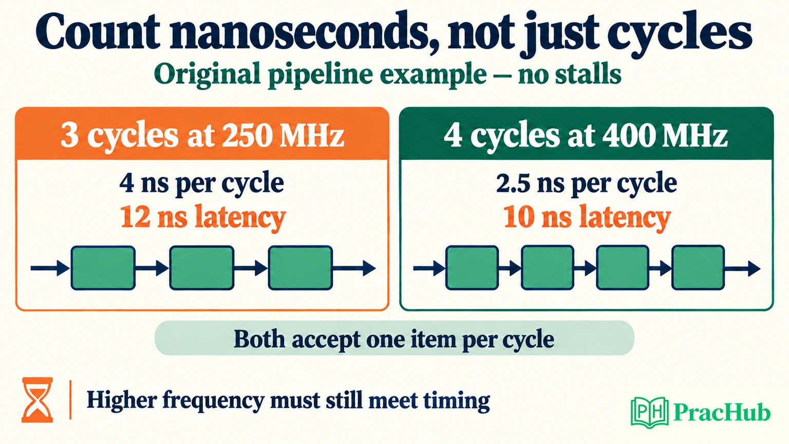
Suppose two candidate implementations perform the same transformation. In this original exercise, latency is measured from the input-acceptance edge to the edge when the corresponding output becomes available. There are no stalls, and both designs can accept one new item every cycle.
| Implementation | Result under the stated assumptions |
|---|---|
| A: 3 cycles at 250 MHz | Period 4 ns; latency 12 ns; capacity 250 million items/s. |
| B: 4 cycles at 400 MHz | Period 2.5 ns; latency 10 ns; capacity 400 million items/s. |
B adds a cycle but reduces elapsed latency by two nanoseconds. It also has greater ideal item capacity because its initiation interval—the number of cycles between accepted items—is one at the higher frequency.
These are separate quantities. Latency concerns one item's journey; throughput concerns how frequently items can enter or leave in steady state. If B could accept an item only every two cycles, its ideal acceptance capacity would fall to 200 million items per second despite the faster clock.
Do not equate these item rates with an Ethernet line rate. That requires the item width, framing, serialization, and interface behavior. Nor does this arithmetic prove that implementation B can close timing on a real device.
Check the timing budget before choosing the faster clock
Primary technical reference: AMD's timing methodology expresses setup slack in terms of the path requirement, maximum data-path delay, clock skew, uncertainty, and setup time. The exact report matters because each contribution can change the result. AMD timing-slack guidance
For a simplified single-cycle path with zero clock skew, assume clock-to-Q of 0.25 ns, logic delay of 2.60 ns, routing of 0.50 ns, setup time of 0.15 ns, and uncertainty of 0.10 ns. The total required budget is 3.60 ns.
At a 4 ns period, the illustrative setup slack is +0.40 ns. At a 2.5 ns period, it is −1.10 ns. Merely requesting 400 MHz does not make the path faster.
Now suppose an additional pipeline register reduces the worst-stage logic delay to 1.20 ns and routing to 0.45 ns, with the other terms unchanged. The stage budget becomes 2.15 ns, leaving +0.35 ns at 400 MHz. This is a plausible arithmetic explanation for the trade-off, not a place-and-route result.
Check all stages, hold constraints, and clocking assumptions before declaring success. Retiming one path can move the worst path elsewhere. If routing dominates, rewriting a Boolean expression may have less effect than placement, fanout, or architectural changes.
Packet-path exercise: define what a fast answer must preserve
Consider an original fixed-format message path receiving 64-bit words. A header identifies the message type and payload length. The block should emit a decoded event only after the required fields have been accepted and validated. Assume the input can be backpressured; this is a toy interface, not a claim about an exchange feed.
Start with four contract decisions. What marks an accepted word? How are partial messages handled? What happens on an unsupported type? What happens if the consumer stalls? Without these answers, “one word per cycle” is incomplete.
For a ready/valid interface, define acceptance as both signals high at the active edge. The source must preserve the pending word while valid is asserted and ready is low. Advance the parser only on accepted words, not merely on elapsed cycles.
A revealing test sends a header, stalls before the payload, then resumes. A parser that increments its field counter during the stall may interpret the payload as a different field. The fastest nominal path is irrelevant if a legal pause corrupts the message.
Add cases for back-to-back messages, reset in the middle of a message, unsupported types, incorrect lengths, and a full output queue. Define whether each case discards, flags, waits, or recovers. Avoid an undocumented mixture of those behaviors.
If you propose cut-through processing, name which decisions can safely happen before the complete message arrives. A field that has not yet arrived cannot influence an earlier result unless the design speculates and defines how it cancels or contains an incorrect action. Keep latency optimization tied to the information actually available.
CDC exercise: a timing exception does not deliver an event
Now move a control event from a 250 MHz source domain to an unrelated 100 MHz destination domain. A one-cycle source pulse lasts 4 ns, while destination edges are 10 ns apart. A pulse that rises just after one destination edge and falls before the next can be missed entirely.
A two-flop synchronizer helps address metastability risk for an appropriate single-bit level crossing, but it does not guarantee capture of every narrow pulse. Explain whether the event can be stretched, represented by a toggle with a bounded event rate, or transferred using a request/acknowledgment protocol. If every event must be preserved, define how the sender knows it can issue another one.
For a multi-bit stream, consider a properly designed asynchronous FIFO and its full, empty, reset, and pointer-transfer behavior. Independently synchronizing every payload bit does not guarantee a coherent word. The correct crossing depends on the information and rate contract, not the number of times you repeat “two flops.”
Primary technical reference: AMD explains that ordinary slack analysis is not reliable for asynchronous clock-domain paths and that suitable timing exceptions are required. Those constraints describe analysis intent; they do not replace a correct crossing circuit or protocol. AMD asynchronous CDC guidance
In a low-latency discussion, quantify the trade-off only after defining the protocol. Synchronization, acknowledgments, and buffering add delay, but removing them without preserving correctness is not an optimization.
Explain verification and performance evidence together
For the packet exercise, maintain a reference sequence of accepted messages and compare decoded outputs against it. Track loss, duplication, order, and payload correctness. Exercise stalls and resets deliberately rather than relying only on random traffic to find them.
Measure latency using the same boundaries used in the design claim. Record the accepted-input event and its corresponding output event, including the matching identifier. Distinguish unloaded latency from latency under backpressure. If a queue can grow, explain the traffic assumption that bounds it.
For a real project discussion, separate simulated behavior, synthesis estimates, post-route timing, and board measurements. Each is useful evidence, but they answer different questions. An arithmetic model like this article's examples does not establish actual device timing or performance.
Bring one case where a measurement changed your design. Perhaps an added register improved the critical path, or a supposedly minor control signal created excessive fanout. Explain your own contribution, the evidence before and after, and the remaining limitation. Do not turn an untested prototype into a production achievement.
Five PracHub questions for targeted preparation
These records combine an Optiver software-role system-design question with cross-company hardware and buffer exercises. They are selected for relevant reasoning, not presented as a verified FPGA assessment bank.
| PracHub question | How to practice |
|---|---|
| Design low-latency trading infrastructure | Locate the latency boundary and explain hardware/software responsibilities. |
| Explain timing and testability concepts | Work through setup, hold, and clock-skew assumptions. |
| Describe common RTL lint warnings and errors | Connect width and structural warnings to circuit behavior. |
| Design signals across power and clock domains | Choose a crossing method from the event and power-state contract. |
| Design a C++ Ring Buffer for Producer-Consumer Use | Rehearse full/empty and wraparound reasoning; distinguish software synchronization from hardware CDC. |
Start with timing and testability practice, then explain the 12 ns versus 10 ns pipeline comparison without confusing cycles, frequency, and throughput. Finish by showing how your packet path behaves when the ideal traffic assumptions stop holding.
Sources and Further Reading
- Optiver Graduate FPGA Engineer, Chicago, 2027 start — official role and location-specific requirements; checked September 8, 2026.
- Candidate FPGA assessment account — August 2026 internship context; not a universal graduate assessment specification.
- AMD: Reviewing Timing Slack — primary reference for the timing terms used in the original exercise.
- AMD: Asynchronous Clock Domain Crossings — primary technical guidance on asynchronous timing analysis and exceptions.
Comments (0)